Thin Wires |
There is only one keyword associated with thin wires. This keyword is provided below.
• THIN WIRE
The thin wire formalism allows the incorporation of thin cylindrical lines with diameters too small to be directly resolved by the finite difference mesh. The basic principle of the formalism involves a transmission line model referenced to the lattice cell boundaries containing the wire. The thin wires can be resistive, inductive, and terminated by an RL series circuit. The presence of the wires is realized in the finite difference code by adjusting the electric fields that lie along the wires, in a manner that simulates the existence and resultant response of the wires. The field adjustments use the wire currents only and therefore the nature of the wires, including the terminations, is not directly communicated.
Many meshed wire segments may exist at the same location, thereby possessing identical finite difference lattice indices, but belonging to different thin wires. In other words, many thin wire segments can pass through the same finite difference cell. However, too many wires within a single cell may result in a numerical instability.
Thin wires can exist within any allowable material in
EMA3D®. This includes linear and nonlinear background materials, isotropic materials, anisotropic materials, and even composite materials. There are many user-selected features associated with thin wires as listed below.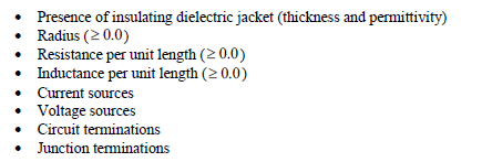
A thin wire can be specified with an outer insulating dielectric jacket. If insulation is desired, then the insulation radius and permittivity must be provided. A bare thin wire is always electrically connected to surrounding material. However, if a thin wire is specified with a dielectric insulating jacket, then the wire is insulated from the material in which it is immersed, except at the wire endpoints. A wire with insulation may therefore, still be terminated at the end points and/or conductively connected to existing material at those endpoint locations.
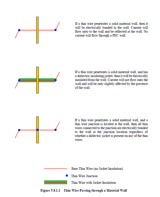
If a bare thin wire passes through a material wall, as shown in the first diagram of Figure 5.8.1.1, then it will be electrically connected or bonded to the material wall. Current on the thin wire will flow directly onto the material wall. If the material wall is PEC or PMC, then a warning message will be issued. The result of such a configuration is zero voltage responses computed at the wall, thereby shorting the wire to the PEC or PMC material at those locations.
If the wire is specified with a dielectric jacket, then the wire is insulated from the wall as seen in the second diagram of Figure 5.8.1.1. The current on the wire will therefore pass through the wall nearly unimpeded. The only effect being a change in the wire impedance at the location of the wall material.
However, if a thin wire junction exists at the wall, as seen in the third diagram of Figure 5.8.1.1, then all thin wires connected to the junction are electrically bonded to the wall at the junction location regardless of whether dielectric jackets are specified.
A thin wire can be comfortably assigned any radius up to 1/10 the size of the smallest finite difference cell dimension in either cross-sectional direction. Exceeding this value may result in numerical instabilities that are manifested by a numerical overflow. However, such instabilities are not always present. Radii as large as 1/6 the size of the average cross-sectional cell dimension, in both directions, have been used often and successfully. If the radius is large and a numerical instability results, it may be eliminated by reducing the finite difference time step. A radius of zero will effectively remove the wire from the problem. If the thin wire radius exceeds ten percent of the cell dimension in either cross-sectional direction, then a warning message will result. If the radius exceeds the cell dimension in either cross-sectional direction, then an error message will result and EMA3D will terminate.
Thin wires are considered perfectly conducting. However, if a resistance is desired, then one may be specified through the resistance per unit length parameter, where the length unit is the meter. All thin wires possess an inherent capacitance and inductance associated with the geometry and the electromagnetic parameters of the surrounding material. However, if additional inductance is desire, such as that associated with lumped inductor circuit elements, then additional inductance can be specified through the inductance per unit length parameter, where the length unit is the meter.
Thin wires can be terminated with simple RL series circuits. These circuits are shown in Figure 5.8.1.2A. Within the circuit diagrams is the material impedance parameter, Zm. This parameter is associated with the material in which the thin wire is terminated. The material impedance parameters are automatically computed.
The last thin wire voltage node is indicated in the diagrams. The circuit resistance and inductance are installed in the last finite difference cell, at the current node location. These resistance and inductance values are put in series with the inherent thin wire inductance and any specified lumped resistance or inductance.
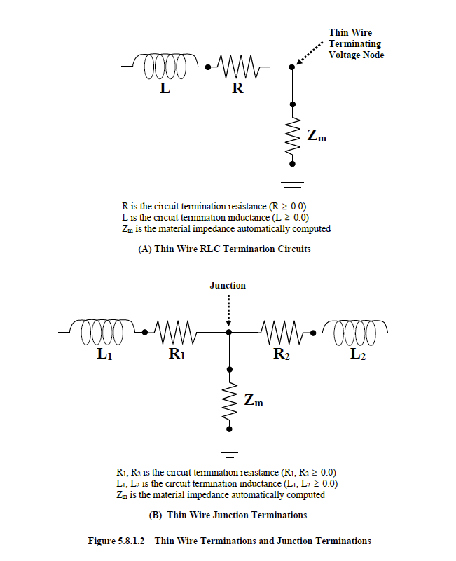
As indicated in the circuit diagrams, a ground is present. This ground is separated from the termination circuit by the material impedance, Zm. The implications of this configuration should be understood. If the thin wire was terminated in air, then Zm is, effectively, infinite in value. If a termination circuit was specified at this termination point, then the values of the circuit termination impedances (resistance and inductance) are, to a large extent, irrelevant. Small or large specified values are masked by the large magnitude of the material impedance. As a result, it is impossible to terminate wires in air with an effective overall impedance of zero. This is advantageous because such a configuration provides a contradictory definition of the wire in the finite difference code. An overall termination impedance of zero implies a grounded wire. Within the finite difference code, however, the wire is terminated in air and ungrounded.
If the thin wire were terminated on a PEC material, then the material impedance is zero and all circuit parameters become relevant. The ground depicted within the circuits of Figure 5.8.1.2A should not be interpreted, in the traditional circuit sense, as a circuit ground, but a bond to the surrounding material at the termination end of the wire.
Thin wires can also be terminated in a junction. A thin wire junction is so termed, when one thin wire is connected to another. Simple RL series circuit terminations can also be applied to wires ending in junctions. The circuit termination at junctions, are interpreted in roughly the same way as those of a single wire termination. The circuit termination for junctions is depicted in Figure 5.8.1.2B.
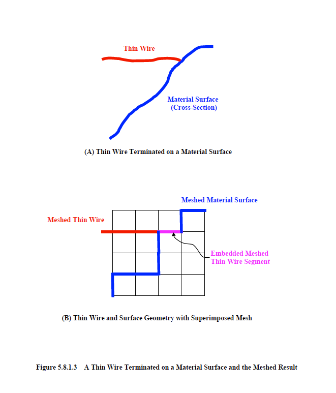
A word of caution concerning the mesh of thin wires is warranted. Thin wires may sometimes be inadvertently meshed into materials. For instance, in Figure 5.8.1.3A is a drawing of the cross-section of a surface and a line designated as a thin wire. The wire is terminated on the material surface. The corresponding meshed geometry is shown in Figure 5.8.1.3B. Inspection of this figure shows the last thin wire finite difference mesh segment to be embedded in the mesh of the material surface. If the thin wire is embedded in PEC material a warning message is issued. The program can be continued or terminated if desired.
If the last segment of a thin wire is inadvertently meshed into another material, the resultant entire wire response is, for the most part, unaffected, unless the wire is terminated in a circuit. If such a circuit termination is specified, then the effects of the circuit will be masked. The degree of masking depends on the electromagnetic parameters of the material. For instance, if the material were PEC, then the circuit termination would be hidden within the PEC material and effectively removed from the wire. The next neighboring thin wire segment would be grounded directly to the PEC material. The effect of the masking increases as the material conductivity or permittivity increases. If there are no circuit terminations, then the only impact is a small change in the effective wire length. However, if a wire current response is specified on the embedded segment, then the result could be significantly different than expected. For a PEC material, for example, the current response would be zero.
The direction or sign of current within a thin wire depends upon the relative positions of the wire beginning point and the wire endpoint, along with the interconnecting thin wire mesh cell segments. However, if a thin wire is defined with a length equal to one mesh cell increment, and there are no other interconnecting segments, then the sign of the current cannot be uniquely determined from the provided information in the EMA3D input file. For an isolated wire with a length of one mesh cell, the wire will be assumed positively directed – that is, the current within the wire segment will be positive if flowing in a positive coordinate direction. However, if the single mesh cell wire segment is connected to other thin wires, then the current signs of the other wires will be queried and the sign of the current within the single wire segment possibly modified.
Thin wires may be driven with current and voltage sources. The current source is an infinite impedance source and sets the current at the location of the source equal to the source value.
EMA3D - © 2026 EMA, Inc. Unauthorized use, distribution, or duplication is prohibited.