EDB Import |
The EDBImport tool lets users use EDB files generated through SIWave or Electronics Desktop. The main features that are imported are the geometry, including dielectrics, vias, traces, and components, which are the RLC passives present in the EDB. The EDBImport automatically assigns materials from the EDB to the geometry and creates point barrier articles to represent the components. This tool allows users to quickly generate a complex model that is ready to mesh and simulate.
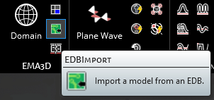
Click the
 EDBImportbutton in the EMA3D section of the EMA3D tab in the ribbon.
In the heads up display, select the EDB Filepath button. See the first table below for a list of Properties and their meanings.
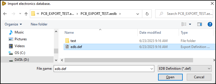
In the pop-up window, navigate to and select the EDB Definition .def file and click Open. Note that the .def file must be in a folder ending with the .aedb extension, which is the default naming convention.
Click OK
 to begin the import. The import process may take several minutes for large, complex files.
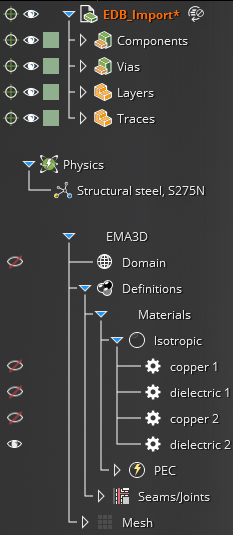
The Simulation Tree will update with the EDB model geometry components, materials, and any definitions that were assigned.
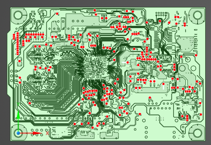
The model geometry and RLC components (red dots, also called barrier articles) will be visible in the model window.
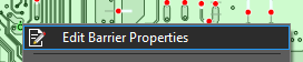
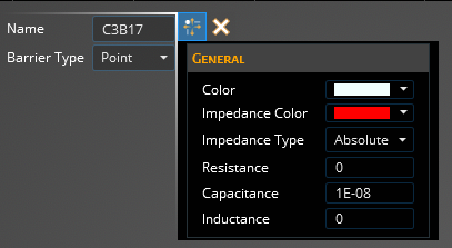
Component values can be viewed and edited by right clicking the component in the simulation tree and selecting "Edit." This will bring up the Seams/Joints tool which more information can be found here
In the heads up display, the name of the RLC component (barrier article) will be visible and the barrier type and other properties can be edited. See the user manual for a list of the properties and their meanings.
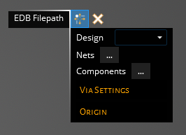
Entry | Meaning |
|---|---|
EDB Filepath | Select EDB file to import. |
Entry | Meaning |
|---|---|
Design | Design to import from EDB file. |
Nets | Opens editor to choose which nets to import. All nets are imported by default.
|
Components | Opens editor to choose which components to import.
|
Use Absolute Tolerance | Switches between using absolute (True, blue) or relative (False, white) tolerance. |
Absolute Tolerance | Absolute tolerance value [mm]. |
Relative Tolerance | Relative tolerance value [% of vias diameter]. |
Use Default Component Height | Use a calculated offset distance for all components. |
Component Height | Set a fixed offset distance for all components. |
X | X location of the origin. |
Y | Y location of the origin. |
Z | Z location of the origin. |
X | Rotation angle about the x-axis. |
Y | Rotation angle about the y-axis. |
Z | Rotation angle about the z-axis. |
Other Resources
EMA3D – © 2026 EMA, Inc. Unauthorized use, distribution, or duplication is prohibited.