Thin Multilayer Surfaces |
Thin surface and thin multilayer surface materials are isotropic materials with a user-defined thickness that is less than or equal to the finite difference cell dimension in the cross-sectional direction. Thin surface materials are not finite difference materials, in the normal sense, but the implementation of a mathematical algorithm designed to simulate the presence of a thin isotropic frequency-independent material.
The thin surface formalism allows incorporation of thin, lossy, or dielectric material surfaces with thicknesses too small to be directly resolved by the mesh. Additionally, the user may define multiple layers of differing properties within the thin surface, so long as the total thickness of the stack-up does not exceed the finite difference cell dimension in the cross-sectional direction. The order of the materials within the stack-up is irrelevant and not considered by the algorithm.
Thin surface materials are characterized by user-supplied values of electrical conductivity (σ), relative permittivity (ε_r), and material thickness (d_c). Permeability (μ) and magnetic conductivity (σ_m) are fixed values with magnetic permeability equal to the vacuum value and magnetic conductivity equal to zero, as specified below:
Assigning permeability and magnetic conductivity values different than those specified above will result in those values being reset to the corresponding correct values. Assigning a negative conductivity value, a permittivity value less than that of vacuum, a negative material thickness, or a material thickness greater than the respective cross-sectional finite difference cell thickness will result in an error message and program termination. Assigning a thickness of zero will elicit a warning message with the thin surface being effectively removed from the problem.
The thin layer algorithm accurately represents the effect of a thin material provided that the sheet depth is much less than the wavelength of the wave propagating in the material (or the wavelength is much greater than the skin depth). Wavelength in a material is inversely proportional to material conductivity, so source excitation bandwidth should be considered when modeling thin conductive materials.
The thin multilayer material algorithm simulates the presence of a material with thickness less than the thickness of an FDTD cell in the normal dimension. This is accomplished via an averaging of the surrounding material parameters with the material parameters of the thin sheet, weighted by the ratio of the thin material thickness to the normal thickness of the cell.
Previous versions of the software have included a thin surface (or composite) material which exhibited numerical instabilities for conductivities less than 100 Mhos/m and did not allow the user to define a permittivity other than that of vacuum. As of 2025R1, the thin surface material has been updated to allow for low conductivities (down to 0 Mhos/m) without issue and to allow the user to define a relative permittivity greater than 1. Additionally, the user may now use the thin multilayer surface feature to define multiple layers of differing properties within the thin surface, so long as the total thickness of the stack-up does not exceed the finite difference cell dimension in the cross-sectional direction.
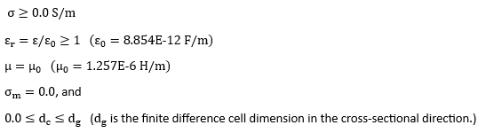
Navigate to the “Structures” drop-down menu within the EMA3D ribbon tab.
Select Thin Multilayer Surface.
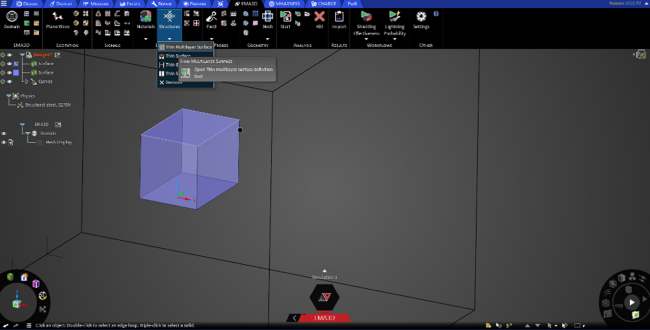
Select the surfaces to which the material definition should be applied. The color associated with this material may be modified in the “Color” drop-down menu.
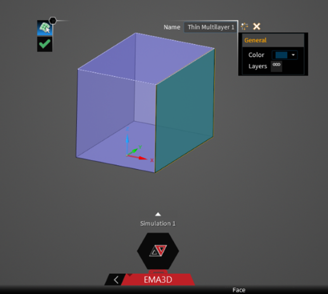
To define the material properties of the stack-up, click the ellipsis button next to “Layers”. A window with a table will appear, in which the user may input the thickness, relative permittivity, and electrical conductivity values associated with each layer. Layers may be added or removed using the “Add” and “Delete” buttons, respectively. When finished, click the “OK” button to close the window.
Once the layer properties have been defined and the surfaces to which those properties should be applied are selected, click the green checkmark to finalize the material definition and exit out of the editing menu.
Entry | Meaning |
|---|---|
Name | Name of the Multilayer Surface |
Entry | Meaning |
|---|---|
Color | Color in which to display the surface material. |
Minimum Thickness | Minimum division thickness [mm]. Number of mesh cells across a layer = layer thickness / Minimum Thickness. |
Layers | - |
Layers | Opens a table to define individual layer thicknesses [mm] and materials in the composite material. Thicknesses must be greater than or equal to Minimum Thickness. |
EMA3D – © 2026 EMA, Inc. Unauthorized use, distribution, or duplication is prohibited.